
PCB engineers layout a product, not only layout wiring, the inner layer of the power plane, but the ground plane design is also very important. Dealing with the inner layer should not only consider power integrity, signal integrity, and electromagnetic compatibility but also need to consider DFM manufacturability.
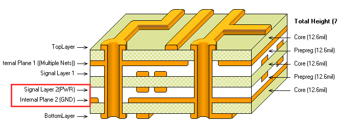
The difference between the inner PCB layer and the surface layer is that the surface layer is used for routing and soldering components, while the inner layer is planned for the power/grounding layer, which is only used for multilayer boards and is mainly used for arranging the power and grounding wires. We call them double-layer boards, four-layer boards, and six-layer boards, usually referring to the number of signal layers and internal power/grounding layers.
Internal design:
The ground layer is designed underneath critical signals such as high-speed signals, clock signals, and high-frequency signals so that the signal loop has the shortest path and the least amount of radiation.
The high-speed circuit design process must consider how to deal with the power supply radiation and interference with the entire system. The general situation to make the area of the power supply layer plane is smaller than the area of the ground plane so that the power supply can play a shielding role. Generally require the power supply plane than the ground plane indented 2 times the thickness of the medium.
- Pyramid Scheme
- Reference Plane
- signal cables cannot be routed across areas
- Power and ground alignment planning
Pyramid Scheme:
The power supply layer plane is adjacent to the corresponding ground plane. The purpose is to form a coupling capacitor and work together with the decoupling capacitor on the PCB to reduce the power plane impedance while obtaining a wider filtering effect.
Reference Plane:
The selection of the reference layer is very important, theoretically the power supply layer and the ground plane layer can be used as a reference layer, but the ground plane layer can generally be grounded, the shielding effect is much better than the power supply layer, so the general preference for the ground plane as a reference plane.

Signal cables cannot be routed across areas:
Critical signals from two adjacent layers must not cross the partitioned area, otherwise larger signal loops will be formed, generating stronger radiation and coupling.

Power and ground alignment planning:
It is important to maintain the integrity of the ground plane and not to run wires in the ground plane. If the density of signal wires is too high, consider running wires at the edge of the power layer.

Inside Manufacturing:
Due to the complex PCB manufacturing process, the inner layer manufacturing process is only part of it, in the production of the inner layer of the board also needs to take into account other processes of the process that affect the inner layer of the manufacturing capacity. For example, pressing tolerance, and drilling tolerance will affect the quality yield of the inner layer.
PCB with different layers can be divided into single-sided boards, double-sided boards, and multilayer boards, these three types of board processes are also very different. Especially multilayer boards, the production process is much more complex than single and double-sided boards. Therefore, when designing multilayer boards, it is necessary to consider the complex process flow of multilayer boards and DFM manufacturability design.
- Delete independent pads
- Inner BGA area
- Internal design anomalies
- Inner Negative Bottleneck
- DFM Inner Layer Design Inspection
Delete independent pads:
Independent pads are non-functional PADs, in the inner layer that is not connected to any network, in the PCB manufacturing process will cancel the independent pads. Because these independent pads canceled on the product design function has no effect, manufacturing will affect the quality and production efficiency.

Inner BGA area:
BGA devices are relatively small and have a very large number of pins, so the fan-out vias are very dense. A certain distance needs to be retained from the drilled holes to the alignment and copper skin during the manufacturing process, otherwise the holes may be shorted in the press-fit and drilling process.

In ensuring that the holes are drilled a certain distance from the copper skin and alignment, the copper in the middle of the holes cannot be retained, which can lead to network open circuits. Therefore, when CAM engineers deal with the BGA area, they need to pay attention to the copper in the middle of the holes and the holes need to be filled with copper bridges to ensure that the network connection is not open after production.
Internal design anomalies:

The holes in the inner negative layer all have hole rings, and the conversion to positive graphics means that all the holes are not connected to the copper skin and are completely isolated. Complete isolation is equivalent to the inner layer does not have any role, do not do the inner layer can be. Manufacturing encountered this problem will confirm with the design engineers, whether the design is abnormal, the inner layer of copper skin does not add a network resulting in complete isolation.
Inner Negative Bottleneck:

When designing the power and ground layer splits in the inner layer, a bottleneck in network conduction occurs due to the density of vias. The copper bridge width of the power network conduction is not wide enough, which will lead to the failure of the matching current, thus leading to the burning of the board. Even some bottlenecks are directly open circuits, resulting in product design failure.
DFM Inner Layer Design Inspection:

NextPCB DFM’s inspection items, for the above-mentioned manufacturability problems, can be detected, and suggest the existence of manufacturing risks, design engineers can use HQDFM to find out the existence of design defects before manufacturing. Design engineers can use HQDFM to detect design defects before manufacturing and modify the detected problem points before manufacturing to avoid problems in the manufacturing process of the designed product, thus improving the success rate of the product and reducing the cost of multiple prototypes.
Faq:
Conclusion:
Designing for manufacturability (DFM) in PCB inner layers ensures high-quality, cost-effective production. By optimizing layer stack-up, trace widths, and clearances, and collaborating closely with manufacturers, you can minimize defects and improve reliability. Effective DFM leads to smoother production, better signal integrity, and lower costs, making it essential for successful and robust electronic products.
Tags : Pcb inner layers explained , Types of PCB layers , Pcb inner layers diagram,PCB layers explained,How to identify PCB layers,PCB layers diagram